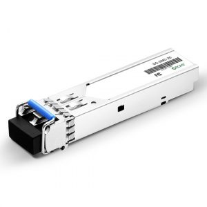
SFP fiber transceiver,1.25G,SM 1310nm,20KM
SFP fiber module,1.25G,SM 1310nm
- Description
- Inquiry
1.25G SFP fiber module Transceiver 1.25G SFP module
1.25G SFP module
(1310nm Single Mode) SFP fiber module
1.25G SFP module Feature:
l SFP fiber module package with LC connector
l SFP fiber module 1310nm FP laser and PIN photo detector
l 550m transmission with MMF
l 10Km~20Km transmission with SMF
l +3.3V single power supply
l LVPECL compatible data input/output interface
l Low EMI and excellent ESD protection
l laser safety standard IEC-60825 compliant
l Compatible with RoHS
Application
- Ethernet
- Telecom
Description:
1.25G SFP module supports dual data-rate of 1.25Gbps/1.0625Gbps and 550 m transmission distance with 50/125 um or 300m with 62.5/125um MF.
The SFP fiber module transceiver consists of two sections: The transmitter section incorporates a VECSEL laser. the receiver section consists of a PIN photodiode integrated with a trans-impedance preamplifier (TIA).
All modules satisfy class I laser safety requirements. The optical output can be disabled by a TTL logic high-level input of Tx Disable. Tx Fault indicates that degradation of the laser. Loss of signal (LOS) output indicates the loss of an input optical signal of receiver.
The standard serial ID information compatible with SFP MSA describes the transceiver’s capabilities, standard interfaces, manufacturer and other information. The host equipment can access this information via the 2-wire serial bus. For more information, please refer to SFP Multi-Source Agreement (MSA)
1.25G SFP module
Performance specifications:
Absolute Maximum Ratings
Parameter | Symbol | Minimum | Maximum | Units |
| Storage Temperature | Tst | -40 | +85 | °C |
| Operating Temperature | Top | 0 | +70 | °C |
| Supply Voltage | Vcc | 0 | +3.6 | V |
| Input voltage | Vin | GND | Vcc | |
| Lead Soldering Temperature & Time | 240/10 | °C/s | ||
Operation Environment
Parameter | Symbol | Minimum | Maximum | Units |
| Supply Voltage | Vcc | 3.15 | 3.45 | V |
| Ambient operating Temperature | Top | 0 | +70 | °C |
| Operating Relative Humidity | – | 5 | 95 | % |
Transmitter Section:
(Ambient Operating Temperature 0°C to +70°C, Vcc =3.3 V)
Parameter | Symbol | Min. | Typ. | Max. | Units | |
| Data rate | – | – | 1250 | – | Mb/s | |
| Center Wavelength | lo | 830 | 850 | 860 | nm | |
| Spectral width (RMS) | Dl | – | – | 0.85 | nm | |
| Average Optical Output Power | Po | -8 | – | -3 | dBm | |
| Extinction Ratio | Er | 10 | – | – | dB | |
| Rise/Fall Time(20%~80%) | Tr/Tf | 0.26 | ns | |||
| Total jitter | Tj | 0.43 | UI | |||
| Optical Eye Diagram | IEEE 802.3z and ANSI Fibre Channel Compatible | |||||
| Input differential impendence | Zdiff | 100 | Ohm | |||
| TX disable | Disable | 2.0 | Vcc | V | ||
| Enable | 0 | 0.8 | V | |||
| Fault | Fault | 2.0 | Vcc+0.8 | V | ||
| Normal | 0 | 0.8 | V | |||
Receiver Section:
(Ambient Operating Temperature 0°C to +70°C, Vcc =3.3 V)
Parameter | Symbol | Min. | Typ. | Max. | unit |
| Data rate | 1250 | Mb/s | |||
| Wavelength | l | 770 | 850 | 870 | nm |
| Maximum Input Power | Pmax | 0 | – | – | dBm |
| Receiver Sensitivity | Pmin | – | -24 | -22 | dBm |
| Output differential impendence | Zdiff | 100 | Ohm | ||
| LOSS Thresholds | LOSSD | – | – | -31 | dBm |
LOSSA | -34 |
EEPROM INFORMATION:
Addr | Field Size (Bytes) | Name of Field | HEX | Description |
| 0 | 1 | Identifier | 03 | SFP |
| 1 | 1 | Ext. Identifier | 04 | MOD4 |
| 2 | 1 | Connector | 07 | LC |
| 3-10 | 8 | Transceiver | 00 00 00 02 12 00 0D 01 | Transmitter Code |
| 11 | 1 | Encoding | 01 | 8B10B |
| 12 | 1 | BR, nominal | 0D | 1250M bps |
| 13 | 1 | Reserved | 00 | |
| 14 | 1 | Length (9um)-km | 0A/14/28 | 10km/20km/40km |
| 15 | 1 | Length (9um) | 64/C8/FF | |
| 16 | 1 | Length (50um) | 37 | 550m |
| 17 | 1 | Length (62.5um) | 37 | 550m |
| 18 | 1 | Length (copper) | 00 | |
| 19 | 1 | Reserved | 00 | |
| 20-35 | 16 | Vendor name | 57 49 4E 54 4F 50 20 20 20 20 20 20 20 20 20 20 | |
| 36 | 1 | Reserved | 00 | |
| 37-39 | 3 | Vendor OUI | 00 00 00 | |
| 40-55 | 16 | Vendor PN | xx xx xx xx xx xx xx xx xx xx xx xx xx xx xx xx | ASC II |
| 56-59 | 4 | Vendor rev | 31 2E 30 20 | V1.0 |
| 60-61 | 2 | Wavelength | 05 1E | 1310nm |
| 62 | 1 | Reserved | 00 | |
| 63 | 1 | CC BASE | XX | Check sum of byte 0~62 |
| 64-65 | 2 | Options | 00 1A | LOS, TX_DISABLE, TX_FAULT |
| 66 | 1 | BR, max | 32 | 50% |
| 67 | 1 | BR, min | 32 | 50% |
| 68-83 | 16 | Vendor SN | 00 00 00 00 00 00 00 00 00 00 00 00 00 00 00 00 | Unspecified |
| 84-91 | 8 | Vendor date code | XX XX XX 20 | Year, Month, Day |
| 92-94 | 3 | Reserved | 00 | |
| 95 | 1 | CC_EXT | XX | Check sum of byte 64~94 |
| 96-255 | 160 | Vendor specific |
Pin Description:
Pins | Name | Discription | NOTE |
1 | VeeT | Transmitter Ground | |
2 | Tx Fault | Transmitter Fault Indication | 1 |
3 | Tx Disable | Transmitter Disable | 2 |
4 | MOD DEF2 | Module Definition 2 | 3 |
5 | MOD DEF1 | Module Definition 1 | 3 |
6 | MOD DEF0 | Module Definition 0 | 3 |
7 | Rate Select | Not Connected | |
8 | LOS | Loss of Signal | 4 |
9 | VeeR | Receiver Ground | |
10 | VeeR | Receiver Ground | |
11 | VeeR | Receiver Ground | |
12 | RD- | Inv. Received Data Output | 5 |
13 | RD+ | IReceived Data Output | 5 |
14 | VeeR | Receiver Ground | |
15 | VccR | Receiver Power | |
16 | VccT | Transmitter Power | |
17 | VeeT | Transmitter Ground | |
18 | TD+ | Transmit Data Input | 6 |
19 | TD- | Inv. Transmit Data Input | 6 |
20 | VeeT | Transmitter Ground |
Notes:
1. TX Fault is an open collector output, which should be pulled up with a 4.7k~10kΩ resistor on the host board to a voltage between 2.0V and Vcc+0.3V. Logic 0 indicates normal operation; logic 1 indicates a laser fault of some kind. In the low state, the output will be pulled to less than 0.8V.
2. TX Disable is an input that is used to shut down the transmitter optical output. It is pulled up within the module with a 4.7k~10kΩ resistor. Its states are:
Low (0~0.8V): Transmitter on
(>0.8V, <2.0V): Undefined
High (2.0~3.465V): Transmitter Disabled
Open: Transmitter Disabled
3. MOD-DEF 0,1,2 are the module definition pins. They should be pulled up with a 4.7k~10kΩ resistor on
the host board. The pull-up voltage shall be VccT or VccR.
MOD-DEF 0 is grounded by the module to indicate that the module is present
MOD-DEF 1 is the clock line of two wire serial interface for serial ID
MOD-DEF 2 is the data line of two wire serial interface for serial ID
4. LOS is an open collector output, which should be pulled up with a 4.7k~10kΩ resistor on the host board to a voltage between 2.0V and Vcc+0.3V. Logic 0 indicates normal operation; logic 1 indicates loss of signal. In the low state, the output will be pulled to less than 0.8V.
5. These are the differential receiver output. They are internally AC-coupled 100Ω differential lines which should be terminated with 100Ω (differential) at the user SERDES.
6. These are the differential transmitter inputs. They are AC-coupled, differential lines with 100Ω differential termination inside the module.
1.25G SFP module
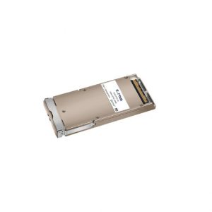
40G module
QSFP+ LR4
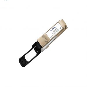
QSFP+ transceiver
100G transceiver
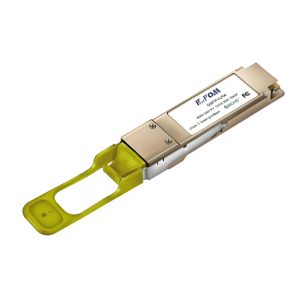
QSFP28 SR4 transceiver
QSFP28 LR4 transceiver
CFP transceiver
CFP2 transceiver
CFP4 transceiver
PDH Multiplexer
SDH Multiplexer
E1 Converter
TDM over IP
Modem
PCM Multiplexer
Fiber Media Converter
Fiber Video Converter
SFP fiber module
Ultra Low Temperature Freezer
Rehabilitation Equipment
Fiber Optical Multiplexer
Related Products
SFP+ Transceiver,10Gbps 1310nm 10Km
SFP+ Transceiver,10Gbps 1310nm 10Km
1.25G BIDI SFP module,20KM,single fiber SFP transceiver
1.25G BIDI SFP module,20KM,single fiber SFP transceiver
SFP+ Optical Transceiver 10Gbps 300m
100Gb/s CFP2 LR4 Optical Transceiver
100G CFP2 Transceiver
100Gb/s QSFP28 LR4 Transceiver
SFP+ Transceiver,10Gbps 1310nm 40Km
SFP+ Transceiver,10Gbps 1310nm 40Km
100G QSFP28 SR4 transceiver
1.25G SFP fiber module,MM,850nm
1.25G SFP fiber module,MM,850nm
40G qsfp transceiver QSFP+ LR4 transceiver
40G QSFP+ LR4 transceiver
single mode QSFP+ LR4 fiber module
40G QSFP+ LR4 transceiver
40G QSFP+ LR4 transceiver
single mode QSFP+ LR4 fiber module